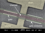
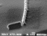
REM-Aufnahme eines Templats für Einzelnanopartikeltransistoren mit einer Kanallänge von ca. 80nm
Inverterschaltungen mit ZnO-Nanopartikeln auf Glassubstrat
Inverter und Dünnfilmtransistoren mit ZnO-Nanopartikeln auf Glassubstrat
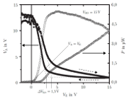
Kennlinien eines Inverters mit Transistorlast; bei den Transistoren handelt es sich um TFT mit ZnO-Nanopartikeln
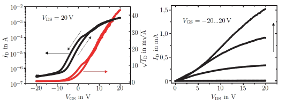
Transfer- und Ausgangskennlinienfelder eines ZnO-Nanopartikeldünnfilmtransistors
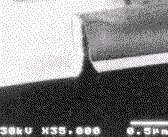
Crystalline silicon structure with 80 nm width at the top and about 800 nm height
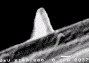
60 nm polysilicon gate structure with the nitride mask on top
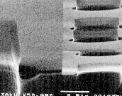
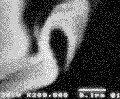
At left a cross section of an oxide structure of 30 nm width on top of a silicon wafer, right top the oxide rings, and right bottom, cross section of an oxide ring structure on silicon substrate
Aluminum line, structured by deposition of PECVD layers
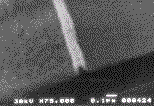
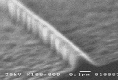
Nanometer scale tungsten line on a 40 nm thick silicon oxide film
MoSi2 line with an oxide mask still on top
TiN line with an oxide mask still on top. The front end of the line is modified by thermal heating of the electron beam in the microscope Nanostructures printed in resist by imprint technique